
COB packaging is a major advancement in LED displays in recent years. Thanks to the development of COB packaging technology, the dot pitch of displays is getting smaller and smaller. At present, high-end LED manufacturers have achieved 0.4mm dot pitch, but The problem is also very obvious. After all, there are some technical barriers, so the price is still relatively high.
COB packaging integrates upstream chip technology, midstream packaging technology and downstream display technology. Therefore, COB packaging requires close cooperation between upstream, midstream and downstream companies to promote the large-scale application of COB LED displays.
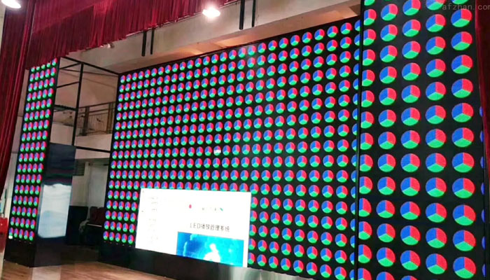
As shown in the figure above, it is a COB integrated packaged LED display module. The front side is composed of LED lamp modules to form pixels, and the bottom side is an IC driving element. Finally, each COB display module is spliced into a design-sized LED display.
The theoretical advantages of COB:
1. Design and development: Without the diameter of a single lamp body, it can be made smaller in theory;
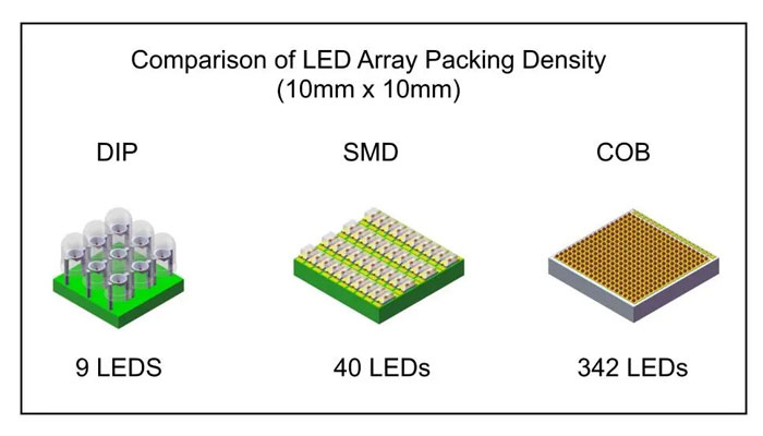
2. Technical process: reduce the cost of the bracket and simplify the manufacturing process, reduce the thermal resistance of the chip, and achieve high-density packaging;
3. Engineering installation: From the application side, the COB LED display module can provide manufacturers of display screen users with a simpler and faster installation efficiency.
4. Product features:
(1) Ultra-light and thin: According to the actual needs of customers, PCB boards with a thickness from 0.4 to 1.2 mm can be used to reduce the weight at least to 1/3 of the original traditional products, which can significantly reduce the structure, transportation and Engineering costs.
(2) Anti-collision and compression: COB products directly encapsulate the LED chip in the concave lamp position of the PCB board, and then encapsulate and cure it with epoxy resin. The surface of the lamp point is convex into a spherical surface, smooth and hard, and resistant to impact. grind.
(3) Large viewing angle: the viewing angle is greater than 175 degrees, close to 180 degrees, and has a better optical diffuse color effect.
(4) Strong heat dissipation ability: COB products encapsulate the lamp on the PCB board, and quickly transmit the heat of the wick through the copper foil on the PCB board. Moreover, the thickness of the copper foil of the PCB board has strict process requirements, plus the sink The gold process hardly causes serious light attenuation. Therefore, there are few dead lights, which greatly extends the life of the LED display.
(5) Wear-resistant and easy to clean: The surface is smooth and hard, impact-resistant and wear-resistant; there is no mask, and it can be cleaned with water or cloth when there is dust.
(6) All-weather excellent characteristics: using triple protection treatment, waterproof, moisture, corrosion, dust, static electricity, oxidation, and ultraviolet effects are outstanding; it can meet all-weather working conditions, and the temperature difference environment of minus 30 degrees to 80 degrees can still be used normally.
It is for these reasons that COB packaging technology has been pushed to the forefront in the display field.
Current technical problems of COB:
At present, COB’s accumulation in the industry and process details need to be improved, and it is also facing some technical problems.
1. The one-time pass rate of the package is not high, the contrast is low, and the maintenance cost is high;
2. The uniformity of color rendering is far inferior to the display screen after the SMD device with light splitting and color separation.
3. The existing COB package still uses the formal chip, which requires die bonding and wire bonding processes. Therefore, there are more problems in the wire bonding process and the process difficulty is inversely proportional to the pad area.
4. Manufacturing cost: Due to the high defect rate, the manufacturing cost far exceeds the small pitch of SMD.
Based on the above reasons, although the current COB technology has achieved certain breakthroughs in the display field, it does not mean that SMD technology has completely withdrawn and declined. In the field of dot pitch above 1.0mm, SMD packaging technology relies on its mature and stable product performance. Extensive market practice and perfect installation and maintenance guarantee system are still the leading role, and they are also the most suitable selection direction for users and the market.
With the gradual improvement of COB product technology and the further evolution of market demand, the large-scale application of COB packaging technology in the interval of 0.5mm to 1.0mm will reflect its technical advantages and value. To borrow a word from industry professionals Say: “COB package is tailor-made for 1.0mm and below dot pitch.”